Call :
PENTA Call 1
Project status :
Completed
Project website :
https://www.project-hades.eu/
Project profile (pdf) :
Project impact (pdf) :
Key application areas
 Transport & Smart Mobility
  Health & Well-Being
  Energy
  Digital Industry
  Digital Life
 Essential capabilities
 Systems and Components
Architecture, Design & Integration Connectivity & Interoperability
 Safety, Security & Reliability
  Computing & Storage
  ECS Process Technology, Equipment, Materials & Manufacturing
PARTNER
CEA / CNRS - Laboratoire d'Informatique de Robotique et Microelec / D4T Systems SA / JTAG Technologies BV / NXP Semiconductors France SAS / NXP Semiconductors Netherlands BV / STMicroelectronics / THALES DIS DESIGN SERVICES SAS / THALES SIX GTS FRANCE / TIMA Laboratory / Institut Polytechnique de Grenoble / Temento Systems SAS / UPMC - Université Pierre et Marie Curie / University of Twente / iRoC Technologies SA
CEA / CNRS - Laboratoire d'Informatique de Robotique et Microelec / D4T Systems SA / JTAG Technologies BV / NXP Semiconductors France SAS / NXP Semiconductors Netherlands BV / STMicroelectronics / THALES DIS DESIGN SERVICES SAS / THALES SIX GTS FRANCE / TIMA Laboratory / Institut Polytechnique de Grenoble / Temento Systems SAS / UPMC - Université Pierre et Marie Curie / University of Twente / iRoC Technologies SA
Countries involved
 France
  Netherlands
 Project leader(s)
Jean-Luc BataillonKey project dates
01 October 2017 - 30 September 2020HADES (Hierarchy-Aware embedded test infrastructure for Dependability and performance Enhancement of Systems) has improved the functional safety of Electronics Components and Systems in order to prevent dangerous failures or to control them as they occur.
Today’s electronic systems require high reliability and functional safety. The “Manufacture and forget” approach has been phased out and equipment vendors are expected to provide support through the entire lifetime of their products. The solution is to use test features to manage reliability challenges, increase operational lifetime and support extended operating environments and dynamic applications.
Background, objectives of the project and challenges
HADES provides solutions for self-test and self-diagnosis of Systems-on-Chips (SoCs) while improving their dependability. More specifically, the project aims at embedding into SoC networks multiple embedded test instruments (ETIs) for both analog and digital Intellectual Property (IP) cores that are interfaced to a common digital test infrastructure. The ETIs equip the SoC with key capabilities such as reliability monitoring to alert the end-users before the failures occur, on-line self-test to detect failures due to latent defects and aging, and data collection for failure diagnosis purposes. ETIs also offer feedback for self-repair, performance optimisation, and reliability enhancement. The goal is to design flexible ETIs that are reusable from post-manufacturing testing to on-line testing in the field of operation.
The test interface is based on the new standard IEEE1687 which has allowed the possibility to build advanced hardware-software environments to monitor and control many different embedded instruments and related applications. Securing the test infrastructure has been of main concern to prevent unauthorised access that could result in stealing secret keys, performing memory dumping, and modifying memory values to get a privilege escalation.
HADES goes beyond the state-of-the-art by moving from a classic design approach, based on a post-silicon fabrication test paradigm, to a new more efficient, scalable and low-cost on-line test approach.
The scope of HADES has been to develop a comprehensive environment to perform the testing of the electronics systems. The range of Electronic Components and Systems (ECS) is very wide, going from transistors in silicon chips acting as individual electrical switches, through the integration in smart systems, up to global System of Systems (SoS) performing complex cognitive tasks and interacting with numerous humans and machines.
A very simplified view of this ECS “stack” or “Russian dolls” is shown in the Figure below:
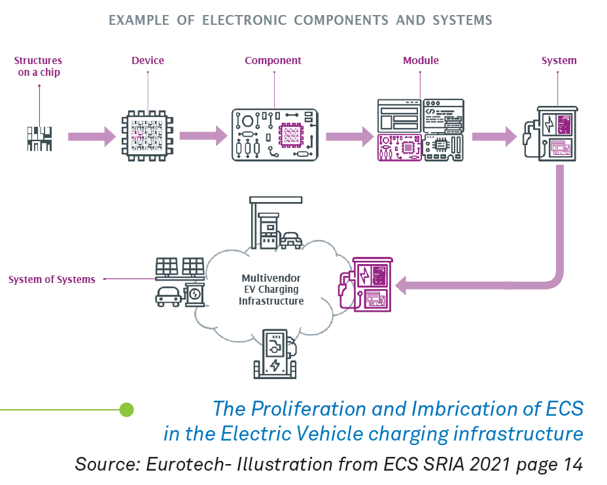
Ensuring the reliability, safety and security of ECS has become a major challenge since the simultaneous demand for increased functionalities and continuous miniaturisation of ECS causes interactions on multiple levels.
Technological achievements
Implementation of the standard IEEE 1687
This required a hierarchical approach for testing all the components of the system. Temento Systems, Tima Laboratory and STMicroelectronics have demonstrated the capability of the IEEE1687 standard to monitor a board and a chip, as well as NXP Semiconductors Netherlands on another demonstrator. They have also implemented a limited pin test interface with an analog test bus, which resulted in the filing of a patent.
TIMA Laboratory, University of Twente and JTAG technologies have developed efficient algorithms and extended their software with IEEE1687 support, achieving scalability, interactive behaviour and lifetime portability.
D4T Systems has developed basic compatibility in their software tools for the new IEEE1687 standard.
Development of Embedded Test Instruments (ETIs)
NXP Semiconductors France and CNRS-LIRMM have developed ETIs that enable testing of Radio Frequency devices using standard digital Automatic Test Equipment. Targeted Application: Smart Home ZigBee Transceiver (2.4GHz) from NXP Semiconductors intended for the IoT market.
TIMA Laboratory and STMicroelectronics have demonstrated an ETI that achieves the static linearity built-in self-test of Successive-Approximation-Register (SAR) analog-to-digital converters (ADCs). A dramatic test time reduction has been achieved.
Université Pierre et Marie Curie (UPMC) newly Sorbonne University has developed low-overhead ETIs for analog and mixed-signal IP cores, also ETIs for fault-tolerance in hardware accelerators for Spiking Neural Networks (SNNs), which constitute the third generation of neural networks aiming at bridging the gap between biology and machine learning.
iROC Technologies has developed a complete library of ETIs and infrastructure for a systematic technology qualification and measurements of the chips. The effectiveness of these ETIs has been demonstrated on CMOS 65 and 28 nm, up to FinFET technologies. An Electronic Design Automation (EDA) platform was built to validate the functional safety of complex circuits targeting ISO26262 certification.
D4T Systems, in collaboration with University of Twente, has developed a new software add-on to quickly analyse the performance of ETIs in a system model simulation.
CNRS-LIRMM and CEA have developed low-overhead ETIs (reliability, area and power overhead trade-off) based on approximate computing circuits to tolerate faults in advanced ICs.
LIRMM and STMicroelectronics have developed a learning-guided approach for diagnosis of mission mode failures. Proposed solution provides reduce and accurate list of candidates to guide the failure analysis phase.
The University of Twente has developed an aging-aware standard cell CMOS library at Spice-level, to simulate the aging of critical paths in processors to locate SD-ETIs. In addition, several AI algorithms suitable for an embedded processor were used to predict in real-time from ETIs, the life-time of a SoC. They also designed, verified and implemented six fully IJTAG-compatible embedded test instruments. Five of them were partly implemented in a 40nm CMOS ASIC and FPGAs.
Security of test infrastructure
The aim is to provide a practical path toward better security by protecting electronic systems test bus access from any evil-minded intrusion while maintaining strict compliance with test standards and without affecting test economics and quality.
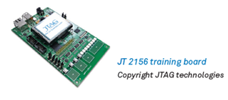
TIMA Laboratory, CNRS-LIRMM and JTAG Technologies have worked on the security of test infrastructure access and Secure Data transfer. They have succeeded in integrating data scan encryption in a standard test flow, successfully implemented on Xilinx boards and on a JTAG Technologies JT 2156 training board.
Some functionalities on a SoC can operate at specific cycle time, while other functionalities may operate at cycle times n/2, n/3, etc. Thales SIX GTS was able to develop a unique Logic built-in self-test (LBIST) on several clock domains, instead of testing each individual domain, by themselves, at that domain frequency. This LBIST will be soon embedded in a big Application Specific Integrated Circuit ASIC (230mm2) taped out in a 65 nm technology.
Thales-Design Services (DIS), ex INVIA, has investigated and developed a flexible ABIST to process internal (CPU driven) or external (Software driven) test, increasing the reliability and security of Integrated Circuits (ICs). It is designed to get a single signature from the test of multiple analog IPs present in an IC. It allows detecting defects or physical attacks in analog modules when the Automatic Built-In Self-Test ABIST system is launched during production test or on the customer side depending on configurations.
Demonstrators
iROC Technologies has developed methodologies and set-ups for complete reliability and functional safety assessment before and during chip design (through EDA) and after chip manufacturing through a test set-up able to submit a chip to multiple variety of tests: radiation, environmental testing as well as hardware fault injection.
A video that shows TIMA laboratory ETI for SAR ADCs static linearity test is available on public platforms: https://hades.iroctech.com/videos/
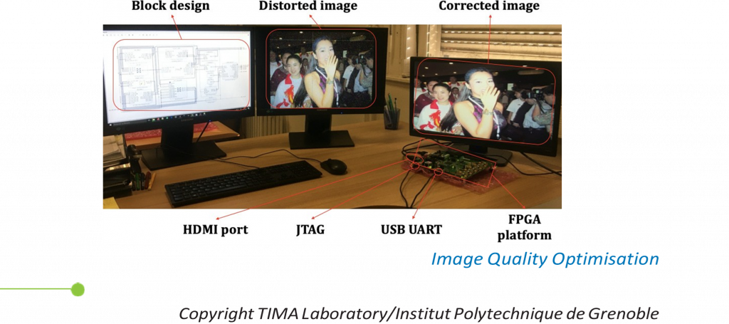
TIMA Laboratory has also developed methods and a digital core for image quality evaluation and optimisation loop for detection and correction of defective pixels in CMOS imagers, paving the way for self-healing imagers.
NXP Semiconductors France and CNRS-LIRMM have developed an indirect test strategy that considerably lowers the cost of the industrial testing phase of RF circuits. This generic framework approach was successfully tested on NXP products and will soon be further extended for the lifetime verification of RF circuits.
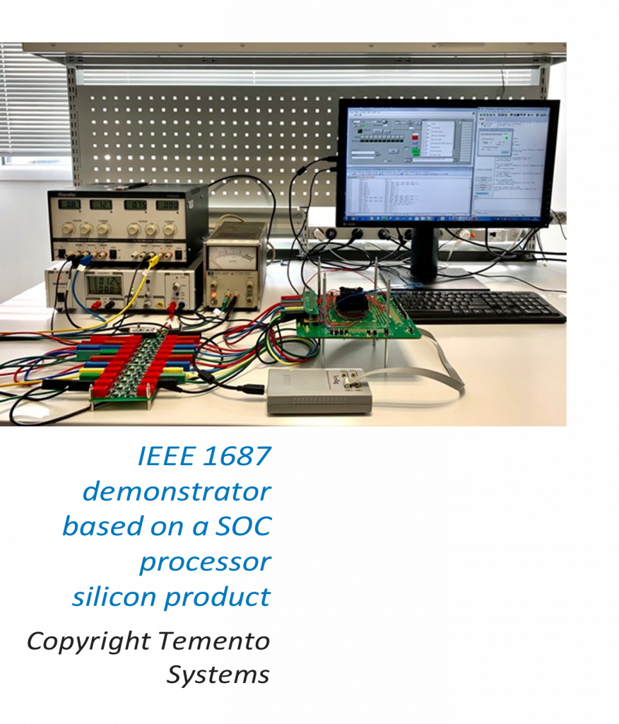
STMicroelectronics, TIMA Laboratory and Temento Systems have developed a 1687 demonstrator based on a SOC processor silicon product. The SoC embeds the state-of-the-art of different elements of the safety mechanism, including the basics like SRAM BIST or more advanced ones like in-situ slack monitors.
Market Potential
With a forecast of more than 40 billion of connected devices in the world in 2025, the market for IOT-dedicated integrated circuits is getting very competitive. Typical examples of such circuits are Systems on Chip that integrate the application processor together with embedded RF front-end. Along with the growth of industrial and home appliances, protocols such as BLE and Zigbee® have become ubiquitous for short-range communicating devices.
NXP is one of the leaders of the home automation and the IoT semiconductor market. To be able to keep this leadership, the testability, quality and features of those products must be improved constantly. The impact of HADES is essential in terms of quality, test cost, time to market, and its results help improve two main fields:
- An auto-test feature is essential to guarantee the proper functionality of safety critical products such as fire detectors, entrance access control, smart metering and even healthcare devices.
- An improved production cost together with new application features help maintain research and development activities in France. HADES innovation is also deployed within other European sites and at NXP worldwide.
The expected impact is the improvement of quality (Parts Per Million) by a factor of 2 for the production test. In term of test cost, a reduction of 30% on test equipment cost is expected, thus improving market share in this highly competitive consumer market.
The automotive transformation will boost the silicon value in the car, which is expected to reach 45 Billion $ in 2023 (Source: IHS – Automotive semiconductor market tracker – June 2020).
The heart of the ADAS applications (Advanced Driver Assistance System) is a system on chip whose ultimate goal is to transform the car into an autonomous vehicle. ADAS has to be 100% dependable and the ETIs developed in HADES demonstrated a proof of concept in hierarchical tests of the SoC that will be a differentiator with respect to the competition.
NXP Semiconductors Netherlands is a major industrial player in the car digitisation and developed an enhanced design automation for on-chip instrument infrastructure using IEEE 1687 ICL. They issued the European patent 82154724 “Limited Pin Test Interface with Analog Test Bus”. The innovation will reduce the test effort by 60%, thereby reducing the time to market and lowering the production test cost.
Thales SIX GTS developed a new LBIST insertion flow, using also the IEEE1687 standard, and the LBIST management module is expected to be reused in future ICs embedded in a range of products delivered by THALES.
THALES DIS, has developed a flexible ABIST controller to process internal (CPU driven) or external (Software driven) test, increasing the reliability (defects) and security of ICs. This ABIST controller will be embedded on secure ICs products, especially when Machine-to-Machine (low defect rate) type of products are required and in secure and certified IPs (used for System On Chip securitisation) type of product.
Spill overs have also benefited SMEs: D4T Systems software solution is positioned between chip design and manufacturing with an impact on more robust, more reliable applications for several high-quality end markets. The compliance to standards makes this new product scalable to other application domains increasing the impact of HADES developments to a wider variety of system products.
JTAG Technologies enlarged the use of their IEEE 1687 tool to reach all the test instruments, and this improvement will further promote JTAG Technologies existing tool chain to support more customers that exploit the IEE 1687 capabilities.
TEMENTO enriched their software existing product with a set of ETIs based on the 1687 standard and demonstrated it while running fault injection.
Exploitation is promising with a first beta site expected in 2021. iROC Technologies currently hold a leading position with their SoCFIT EDA platform and new capabilities have been added, targeting the certification for ISO26262 Tool Confidence Level 3, key to address the electrical cars and ADAS market. 2 to 3 new licenses per year are expected.
Societal & Economic Impact
The semiconductor total available market grew by 7.3% in 2020 compared to 2019, despite the Covid-19 pandemic and the political conflict between the United States and China. This demonstrated to politicians, key decision-makers and the general public that semiconductors are a Key Enabling Technology in a digitised society. More and more cars are now equipped with several image sensors and algorithms, powered by artificial intelligence to capture the environment around the car and take action, like emergency breaking. Such features will have to be adopted by a large majority of drivers if the objective is to move to autonomous driving, and the sine qua non condition is to develop electronic system and software with a 100% reliable functional safety that, for example, will be able to alert the driver and pull over the vehicle in case of a failure of the autonomous driving controller.
The quality, reliability, safety and cybersecurity of electronic components and systems are, and will be, fundamental to a society that is more and more digitised This key domain of the ECS was strengthened by HADES, as well as the technological leadership of the involved partners.
Similarly, the research organisations, e.g. CNRS-LIRMM, Sorbonne University, TIMA Laboratory, and University of Twente, have gained valuable knowledge working together and with industry towards functional safety solutions for microelectronics. Some of the material that was developed during the course of the project is already included in M.Sc. programme curricula of Universities in France and the Netherlands. Research organisations have also offered several tutorials in international conferences and summer schools on topics related to the project. 14 PhD theses have been carried out within the framework of the project, enhancing significantly the labour force in this domain.
Patents/Standardisation/ Publications
The project results from HADES featured strong dissemination activity and achieved considerable publicity, targeting high-impact and world-class conferences and journals. 56 international conference articles, 17 journal articles, 17 workshop articles were published, together with 8 invited talks and 6 keynote talks presented in conferences. The project results were presented at EFECS 2020, with posters and videos made available in the virtual booth. The partners also delivered a Special Session dedicated to the project at the IEEE conference IOLTS’20.
The implemented innovations are protected by 3 patent applications:
- NXP Semiconductors Netherlands European Patent 82154724 “Limited Pin Test Interface with Analog Test Bus”
- TIMA Laboratory: M Portolan ”Test apparatus and method for testing an integrated circuit”. Patent No. FR3066606A. 23 March 2018.
- CEA: M. Seif and V. Gherman, “Device And Method For Controlling Refresh Cycles Of Non-volatile Memories”, FR1658135 (070550 US FLO/VBO)
3 MSc thesis / 14 PhD dissertations were produced.
NXP Semiconductors NL was active in IEEE P1500, IEEE P1687.1 and IEEE P1687.2 workgroups to drive third party silicon IP and EDA. iROC Technologies is a member of French ISO 26262 committee and a member of the Working Group for the JEDEC JESD89B revision. University of Twente was also very active in TESTA (TEst STandard) workshops on (mixed-signal) IJTAG (IEEE 1687.1/2) standardization. TIMA Laboratory participated in the leading standardisation proposal for support of non-JTAG interfaces inside the IEEE P1687.1. Sorbonne University was active in the working group activities of the 2 standards IEEE P1687.2 (Standard for Describing Analog Test Access and Control) and IEEE P2427 (Standard for Analog Defect Modelling and Coverage).
Future Developments
Today, most applications and standards in the electronics components and systems domain require high reliability, security and functional safety. As such, the topics explored in HADES are, and will be, fundamental to digitised society.
HADES can be considered a precursor project and the numerous activities & innovations demonstrated in HADES established the foundations for going even further to develop new disruptive applications related to electrical cars and ADAS, Advanced Space missions and Medical – especially Implantable devices. The markets in these 3 sectors, in which Europe already has a strong share, will experience spectacular growth.
Novel ETIs will be needed to focus on automated intelligent insertion, using on-chip Intelligence techniques based on Machine Learning, to extend the applicability and usefulness of physical data. The support of new and upcoming standards for the IoT, for reliability, for functional safety, for security, such as ISO 26262, IEEE P2851, IEEE 1687, will need close collaboration among all players to build leadership going forward in this coming generation of advanced Components and Electronic Systems.
Novel Software and EDA are needed to manage FuSa/R and complexity of novel applications:
- Massive use of Machine Learning techniques
- Introduction of a novel concept “Design for Functional Safety and Reliability (FuSa/R)”, in line with the existing DFM/DFR (Design for Manufacturing/Reliability)
- Sensor data fusion for data presentation.

