Project status :
Recently completed
Project profile (pdf) :
Project impact (pdf) :
Key application areas
 Semiconductor Fabrication
 Essential capabilities
ECS Process Technology, Equipment, Materials & Manufacturing Countries involved
 Switzerland
  Germany
  Netherlands
 Project leader(s)
Bernd SrockaKey project dates
01 March 2020 - 31 December 2023Europe’s open, multi-application platform for wafer production with onsite configurability.
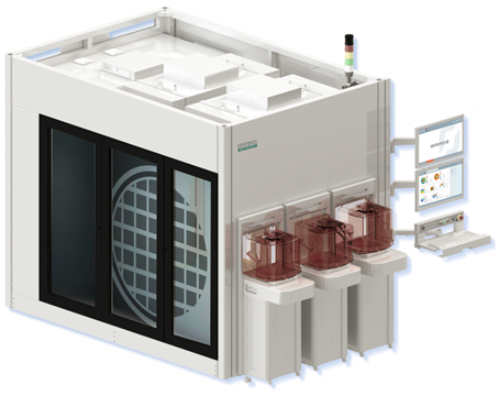
The Wafer Metrology Centre project provided an open and highly modular hardware metrology platform with up to 10 parallel and easy in-field exchangeable sensors for a wide range of wafer metrology applications.
Current metrology tools are often too monolithic and can’t be reconfigured to various and fast-changing needs. The Wafer Metrology Centre project was aimed to bring much more flexibility by creating a multi-sensor, highly and in-field adaptable hardware platform including also new sensor ideas. Providing the space and the appropriate environment for the different sensors while keeping tool and software compact was a challenge.
Achievements and results
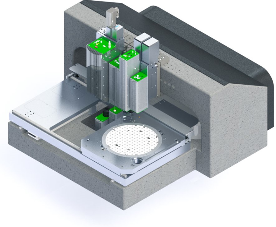
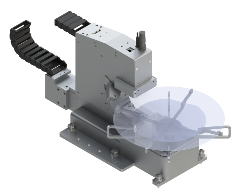
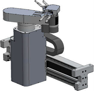
With the WMC project partners have developed an industry open, modular wafer metrology platform for a wide semiconductor application range. It carries up to 10 different sensors in parallel either in-house made or even from other vendors by its standard interface. This platform provides easy in-field exchangeability of different sensors. Hence the WMC can be configured to measure various parameters and 3D-profiles of semiconductor wafers simultaneously and can also quickly follow fast-changing needs by re-configuration. Also new ideas of high-speed profiling and film thickness sensors have been brought to a prototype level.
Background, objectives and challenges
Current semiconductor metrology and inspection tools are often too monolithic and can’t be reconfigured to the many different and fast-changing requirements of emerging products. Equally important, this lucrative market is currently dominated by five large companies, none of which being European. The new WMC shall provide such a platform, not only flexible in functionality and application, but also providing a ‘framework’, open in its approach to business, operational process and technology. The WMC business model is aimed to attract innovative metrology companies in the field of optical-sensor techniques, as well as semiconductor customers. Sensor vendors benefit from a technology, sales and distribution platform, while users from a flexible, scalable, multi-application and cost-effective tool. Operational processes, open and modular in concept, will deploy multiple sensors in a wide range of applications, which can be combined and retooled onsite – a unique capability in the semiconductor market.
Project technology innovation covers: Modularity in use and retooling of sensors requires a lot of engineering in hard- and software since sensor and automation components must be configurable, metrology recipes need to be combined and linked and a standardised Interfaces is needed. The same modularity is required for the wafer-handling to make this ‘generic’ platform deployable for various applications in the semiconductor value-chain.
New metrology capabilities have been part of the project:
- Extension of a digital holography microscope to a much larger field of view to speed up the 3D-profiling.
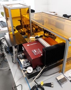
- Mid-infrared reflectometry to be used to measure film thicknesses not possible in the visible range.
- A super-fast multi-wavelength interferometry profiler is intended to scan full wafers with thousands of contact pillars in less than 2 minutes.
- Extended depth of focus camera technology to allow for getting images from structures with large height changes within a single shot.
Technological achievements
Within the Wafer Metrology Centre project, the consortium developed a unique modular hardware platform configurable for various applications. It can measure wafers both from top and bottom side and may use up to 10 parallel mounted sensors of a variety of optical metrology technologies. All of them
are made to be easy in-field exchangeable. Data streams from all the sensors may be combined and evaluated within the tool software to give more comprehensive insights. In the automation section we developed the industry first robot, which is capable to flip wafers with both hands, giving a throughput advantage and makes recipes easier. Furthermore, it can automatically exchange the handling hands to adapt to different wafers and frames. The same flexibility could be achieved with the new designed pre-aligner, able to manage very different wafer edge features.
The project also developed specific measurement sensors. In particular, it significantly enhanced the stability and homogeneity of digital holography over a large field of view, to allow single shot profiling of areas as large as a full lithography-shot with nm height resolution. In the mid-infrared range our demonstrator measures the spectra of light reflection about 100 times faster than currently available systems. Also, with our approach this speed doesn’t shrink with spectral resolution like in other common techniques. This will greatly enhance abilities for film thickness & structural metrology for new emerging materials. A proof of principle demonstrator could be created for a very high-speed 3D-profiler using several wavelengths and deploying an interference technique. It is intended to map contact structures (bumps and pillars) in the range of few microns size over the full wafer surface within less than 2 minutes. Complex correction mathematics had to be implemented to get rid of all the optical issues connected to these small, often mirror ball like features. Overall, a great step could be done to enhance wafer metrology in the direction of modularity and easy task adaptation.
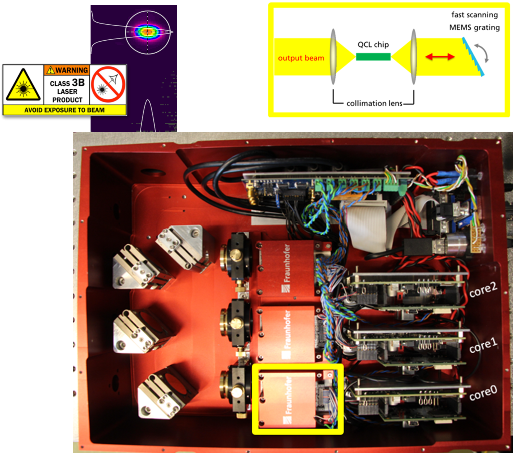
(Copyright: Fraunhofer IAF)
Market Potential
Building upon the project achievements, the consortium plans to bring the Wafer Metrology Center tool to the market before the end of 2024. They already attracted substantial interest; due to the performance enhancement that they could achieve with the WMC-demonstrator. Sentronics expects in 2024 a revenue growth of more than 20% and could secure already till end of 2023 bookings which are 1.6 times the 2023 revenue. The new sensors developed contribute additionally to portfolio extensions for all company partners, especially in the field of high speed 3D-profiling. For the Mid-IR-sensor the consortium already started a follow-up project to industrialize the laser core manufacturing, which will open a large market in medicine, pharma, chemistry, environment, and other fields beyond semiconductor applications.
Societal & Environmental and Economic Impact
With the WMC project, the consortium tremendously increased the flexible adaptability and re-useability of the platform base, as a direct contribution to environmental footprint reduction by avoiding new platform manufacturing for every new task. This is an important step for the transition from existing more monolithic metrology products to the new platform idea. The WMC project could help European companies to get leadership in that market. Finally, the consortium initiated the creation of an ecosystem of European high-tech companies and Research Centres which will continue to co-operate beyond the project.
Patents/Standardisation/ Publications
In preparation of the WMC project, two patents dealing with high-speed interferometry based 3D-profiling have been filed already during the application phase. The project results have been published in 6 conference presentations and journal publications, where two more are planned. The consortium took part in 5 industrial resp. scientific exhibitions. Three new projects are started or are planned to start using results of the WMC project.
Future Developments
The consortium will continue the integration of multiple new sensors into the WMC. For the mid-IR laser sources, they started an assembly automation project including also a more advanced digital electronic. The holographic profiling will become fully integrated into the WMC and add single-shot, single nm height resolution 3D-profiles ability. The volume diffraction grid development as the essential part for the wide field-of-view sensor configuration is continued. The interference based high-speed 3D-profiler will go into the prototype phase, where they plan to achieve their speed and resolution targets.

