Call :
PENTA Call 1
Project status :
Completed
Project website :
http://hybman.eu/
Project profile (pdf) :
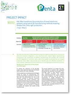
Project impact (pdf) :
Key application areas
 Digital Industry
  Digital Life
 Essential capabilities
 Systems and Components : Architecture, Design & Integration
  ECS Process Technology, Equipment, Materials & Manufacturing
PARTNER
Eindhoven University of Technology / Fraunhofer-Gesellschaft zur Förderung der angewandten Forschung e.V. / Henkel AG and Co KGaA / Neotech AMT GmbH / Reden BV / Robert Bosch GmbH / Signify / TNO / Technolution BV / VSL BV / XENON Automation GmbH
Eindhoven University of Technology / Fraunhofer-Gesellschaft zur Förderung der angewandten Forschung e.V. / Henkel AG and Co KGaA / Neotech AMT GmbH / Reden BV / Robert Bosch GmbH / Signify / TNO / Technolution BV / VSL BV / XENON Automation GmbH
Countries involved
 Netherlands
  Germany
 Project leader(s)
Rob van AsseltKey project dates
1 April 2017 - 31 March 2020Hyb-Man transforms the production of smart electronic systems using hybrid 3D manufacturing methods enabling flexible first-time-right production.
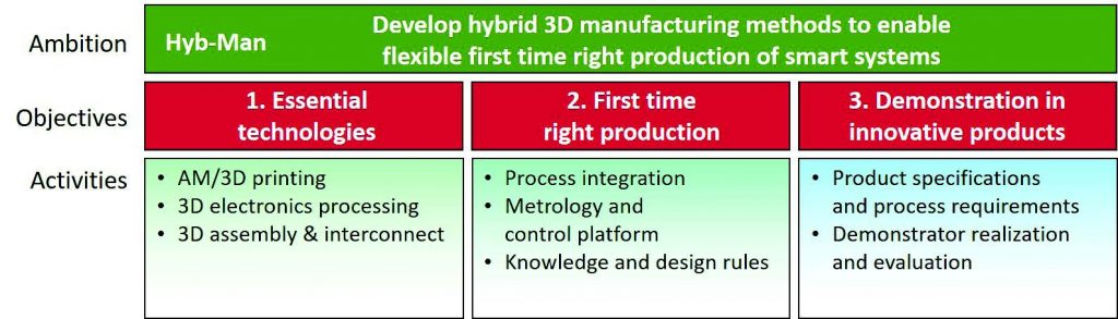
Hyb-Man develops hybrid digital manufacturing technologies to produce three-dimensional electronic functions integrated in the structural parts. Hybrid digital manufacturing encompasses the combination of additive manufacturing (3D printing) with assembly and 3D integration of electronic parts, and in-line quality monitoring into one integral production chain. Major opportunities are in flexible and cost-effective production of smart systems, enabling customised electronics for new lighting and automotive products.
Background, objectives of the project and challenges
To achieve the ambitions of the Hyb-Man project, three objectives have been formulated which address the major challenges.
The first objective is to develop the technologies needed for hybrid 3D manufacturing. This includes 3D printing of mechanical structures that meet the requirements for use in end products, printing of electrical structures in horizontal and vertical directions, and placement and electrical connection of standard components such as LEDs and sensors. Special emphasis is on the mutual compatibility of the technologies, and the inclusion of methods to monitor the progress and quality during manufacturing. The second objective is to enable first-time- right production of systems with integrated mechanical and electrical functionality. First- time-right refers to both product designs and controlled processes. This requires deep understanding of the relation between the product properties and the processes, documented in design guidelines. This understanding is created by a combination of numerical modelling and process investigations. Process control is achieved by the integration and combination of various technologies in the proper way, including methods for in-line inspection and control.
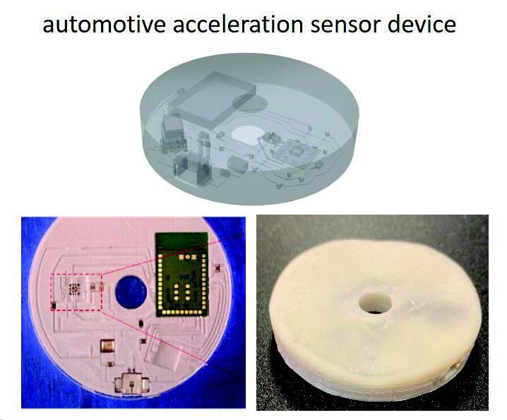
The third objective is to demonstrate the hybrid 3D manufacturing approach in two innovative product cases: LED lighting and automotive acceleration sensors. The specifications of these products determine the technology requirements. Dedicated product designs are made, which fit with the selected technologies. Products are manufactured and evaluated against the requirements. This includes environmental and stress testing, to mimic the long-time use in actual products.
Technological achievements
Hybrid manufacturing technologies, materials and processes
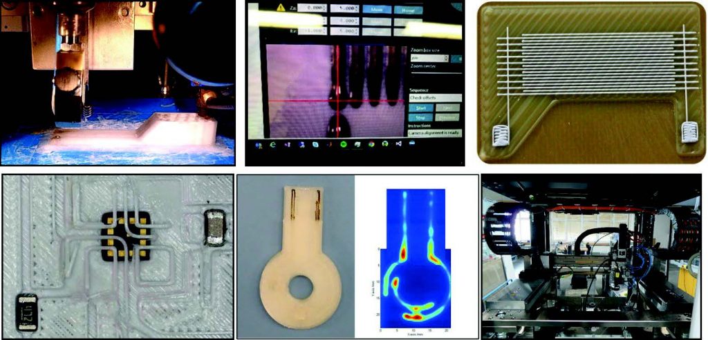
Technologies to print electronics in 3D developed in the project, resulted in new and improved processes and materials. 3D printing structural materials based on extrusion (FFF) and photo- polymerisation (SLA), were combined with pick and place (P&P) of standard components, and direct write techniques of curable conductive inks and pastes. Better process understanding was generated to allow printing of fully integrated three-dimensional systems, and to improve process stability and reproducibility.
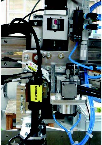
Metrology and in-line control technologies
In-line inspection and control methods were developed, including contactless resistance measurement based on Eddy-current sensing, and a vision-based pick and place system for component embedding.
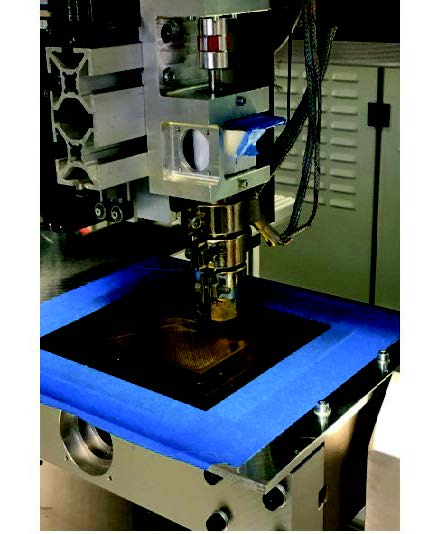
Manufacturing systems combining 3D printing, printed electronics and pick & place
The partners successfully implemented these new technologies into two prototype manufacturing systems, based on FFF and SLA technology combined with P&P. These systems can produce functional electronic products that are completely hybrid manufactured. Monitoring and control have been implemented for integrated temperature control, level sensing and camera inspection.
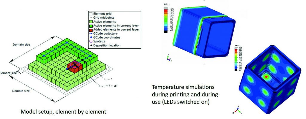
Modeling and design rules
Simulation tools and strategies have been developed to model mechanical properties, stress, and temperature profiles during printing and product use. The models are dynamic and add elements in time, like in 3D printing, and achieve the right level of accuracy which is validated by experiments. Basic design guidelines are explored by implementing exemplary cases in the Reves design exploration software.
Demonstrators: automotive, LED lighting
LED lighting and automotive demonstrators including embedded tracks, connectors, LEDs, sensors and Bluetooth modules have been made by both process routes. The key electrical and geometrical properties have been reached: conductivity up to 20% of bulk copper was achieved, which is suitable for medium power applications.
(Bosch, Neotech, TNO, Signify, Fraunhofer IFAM)
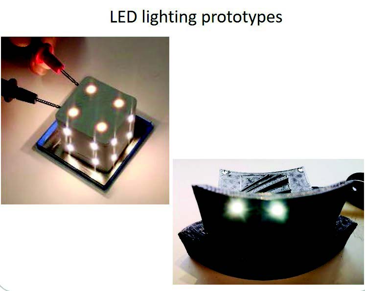
The project demonstrators have been used extensively: they are well received and clearly show the properties and opportunities to various stakeholders. Several ideas for further improvement of processes, designs and applications have been generated, to make the next step towards end-user products that benefit from the design freedom enabled by 3D embedded electronics
Market Potential
Additive manufacturing and 3D printed electronics markets are forecasted to grow 13-26% per year up to 2028. The 3D printing electronics market is still small and will grow as technology matures, cost is reduced, and technical specifications are met.
Up to now significant interest has been raised for the Hyb-Man demonstrators, materials, process chains, process control and modelling methods. The innovation achieved reinforces the competitive position of all partners in 3D printed electronics. Neotech has received first requests for R&D production systems and Technolution has started deploying parts of the control platform in customer projects.
The Hyb-Man market impact is expected to reach 10-100 M€ per year, based on:
- end products for automotive (Bosch), LED lighting (Signify, extension of 3D printed LED lightings), as well as other applications
- new materials (Henkel, Fraunhofer IFAM), processes and equipment (Neotech, Xenon, TNO)
- metrology (VSL) and control platforms (Technolution) to improve process control
- modelling tools and support (Reden, TU Eindhoven)
Societal & Economic Impact
The Hyb-Man project enables the capability to bring electronics manufacturing back to Europe, by mastering a complex set of technologies. We brought together material, process, modelling, and design expertise from different partners to develop the combined technologies to the next level. Together the partners have created an eco-system which covers the complete value chain of materials, equipment, product manufacturers/OEMs and end users, which is key to realise commercial manufacturing and to drive market adaptation of 3D embedded electronics. This eco-system provides Europe with a world-leading position which will be difficult to replicate. Economic growth in Europe is further driven by the fact that the manufacturing processes are first- time-right and highly digitised, enabling cost-effective local production of high- tech electronic products in small series.
During the project an end to end approach towards first time-right production has been developed, from material to process to simulation to product. The Hyb-Man partners have demonstrated technical leadership in their field of expertise, which helps to attract talented scientists, designers, developers, and partners, thereby driving further economic growth and impact. In the coming years 7-10 new job positions per year are anticipated in the areas of material and process development, manufacturing, product design, process control, simulation tools and software. This number will increase when applications expand to other areas.
Hyb-Man also creates significant environmental benefits, because material usage is reduced, less transportation is needed due to local production, products can be recycled, and materials reused at end of life. Material usage is reduced by first-time- right production (no need for multiple print runs and less process failures), product designs optimised to achieve the functionality with minimum amount of material, and products made to order (no obsolescence or waste of products on stock).
Consumers will benefit from these developments by getting access to new smart products with additional capabilities, new form factors and a reduced environmental footprint.
Patents/Standardisation/ Publications
The partners actively disseminated the project results at various events, including large conferences such as IDTechEx, LOPEC and Productronica/ Semicon. In total 58 events were visited, and 42 oral presentations given. The know how created in the project has resulted in three patent applications.
Products manufactured by the new hybrid manufacturing methods will follow existing standards for e.g. LED lighting and automotive applications.
Future Developments
- The great progress and insights generated in Hyb-Man resulted in the aim to evolve into a follow-up project, to move forward in the following areas:
- Use of functional materials and material combinations to further increase integration of electrical, mechanical, and optical functionality.
- Process industrialisation towards scalable volumes, reduced cost and cycle times, and closed loop control.
- Improved models, faster calculations and integration of simulation and design software.
- New applications that benefit from customisation and miniaturisation, using improved 3D electronics design tools and easier conversion to process settings.

