Call :
PENTA Call 3
Project status :
Running
Key application areas
 Computing and Storage
  Security and Reliability
  Digital Industry ECS Process
  Transport and Smart Mobility
  Equipment, Materials and Manufacturing Safety
 Essential capabilities
 Systems and Components Architecture, Design & Integration
Connectivity & Interoperability
 Safety, Security & Reliability
  Computing & Storage
  ECS Process Technology, Equipment, Materials & Manufacturing
PARTNER
EXTOLL GmbH / Fraunhofer-Institut für Zuverlässigkeit und Mikrointegration / GLOBALFOUNDRIES Dresden Module One LLC and Co KG / HTWG Konstanz - University of Applied Sciences / Hyperstone GmbH / Racyics GmbH / SiliconGate LDA / TIEMPO SAS
EXTOLL GmbH / Fraunhofer-Institut für Zuverlässigkeit und Mikrointegration / GLOBALFOUNDRIES Dresden Module One LLC and Co KG / HTWG Konstanz - University of Applied Sciences / Hyperstone GmbH / Racyics GmbH / SiliconGate LDA / TIEMPO SAS
Countries involved
 Germany
  Portugal
  France
 Project leader(s)
Richard WillemsKey project dates
15 November 2019 - 31 May 2024XSR-FMC project developed a very reliable, secure and ultra-low power flash memory controller using a European supply chain.
NAND-Flash based storage solutions are used in many devices of our daily life. Looking to professional applications like industrial, medical, NetCom or automotive applications, the storage system must be extremely reliable and secure since it is often the backbone of the business. More than 2% of the global energy is used just for data storage, which makes the demand clear to develop a very power efficient system. The goal of this project was a fully running PCIe SSD demonstrator, based on technologies available as much as possible in EU.
Achievements and results of the project
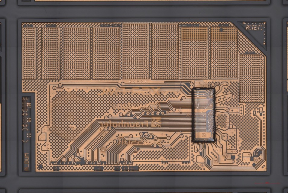
Within the project a dozen IPs were developed, which are now listed in the foundry IP catalog. Most of these IPs are of a high complexity. To validate them, 3 MPW (Multi Product Wafers) were realized, and a FPGA based prototyping system was set-up. Two patents were filed, 9 journal articles were published and presented at 10 conferences. With Thin-Flex embedded a new packaging technology reached the prototype phase. Not to forget the developed firmware, which orchestrates the entire system. The IPs are needed in the system context, as for example different sensors (e.g. temperature, voltage) are essential to keep the storage system in defined conditions.
Background, objectives of the project and challenges
Data storage, using NAND Flash, is used in many professional applications. In the past the “industrial” applications were more legacy like, using form factors like USB, SD or eMMC. 5G/6G NetCom application, plus autonomous driving, have at least the same reliability needs, but require higher data rates in combination with security and safety aspects.
The political discussions of the last years showed that information technology is of national/EU interest. Therefore, a controller developed in the EU and to establish a European engineering- and production chain was a defined project target. The development of a NAND flash-based storage system requires special know-how in various categories, starting with system architecture and ending up with PCB and production related topics. Looking just a bit more to the details, a lot of specialized IPs are needed, which must all fit in to the system
context. An early question to answer was which semiconductor technology is best suited? The decision to use the 22nm SOI technology was an easy one. This technology has with ABB (Advanced Body Biasing) benefits in the triangle of power- performance- cost. Furthermore, this technology is by a factor of magnitude better in terms of alpha particle resistance. Finally, the production is in Germany.
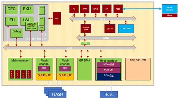
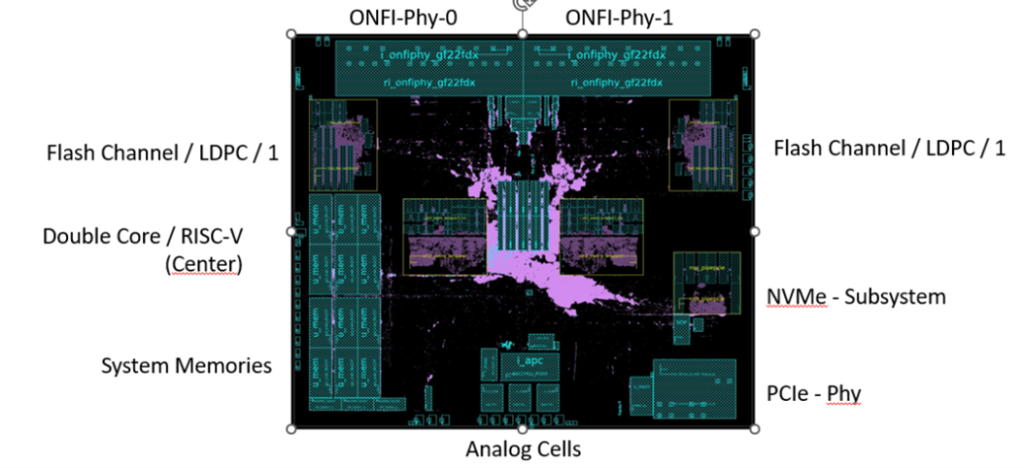
Racyics made their ABB library available for all partners. Extoll developed the PCIe Gen4 Phy and integrated the PCIe controller IP. The data throughput for one flash channel was defined of up to 1.6GT/s. In this range optimized Pads are not suited, which is the reason why an Onfi Phy system was developed.
To supply and to control the system with the right voltage level, SiliconGate developed a set of analogue IP. A flash controller cannot be reliable without a powerful Error-Correction-Code (ECC). HTWG Konstanz did investigations for the best-suited algorithms (performance, power, area). They also analyzed the bit errors, to understand in detail the flash behavior. The
developed algorithms were later used in the context of post-quantum cryptography. Fraunhofer IZM looked for packaging technology. Thermo-mechanical simulations were done and with Thin-Flex Embedding a new packaging technology reached the prototyping phase. Tiempo-Secure designed a complete Secure Element with a secured RISC-V architecture, that has been prototyped on the GF 22nm SOI process and that successfully completed a Common Criteria EAL5+ AVA_VAN.5 security evaluation. The top level design and firmware development
happened at Hyperstone.
Technological achievements
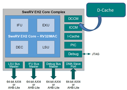
In this project more than a dozen IP was generated, including two high speed PHY’s. Beside the mentioned ones three different RISC-V implementations were used in the project. The most powerful one is a 9 stage, dual thread, multi core solution, based on the open EH2 implementation, but with a couple of enhancements and a lot of verification spent. In general, a completely new platform for a next generation flash controller was developed. This platform is easier scalable and can be used in combination with other interfaces like UFS or similar. The controller can support the latest flash technologies, supporting the Onfi and the ToggleNand standard. The ABB library from Racyics helped a lot to reduce the power. For the main contributor to the cell area, the LDPC engine, the leakage was reduced by 85% compared to a zero-body-biasing approach. With MRAM a new technology was used by Tiempo-Secure. The positive experience reduces the hurdle for all partners to use this technology in their future product developments. It wasn’t foreseen that HTWG Konstanz gets active in the security domain. Their investigation in the ECC domain brough new idea how Post Quantum Cryptography could be realized in a very efficient way. Since security was one key aspect of this project, changing the focus from ECC to security was a very good decision. Fraunhofer IZM helped in two ways. With their thermos mechanical simulations they gave an inside that is very useful for the physical design of an SSD drive. With Thin Flex Embedding a future oriented packaging technology was developed, which is of interest for ultra-thin form factors like μSD or similar.
Starting the development of a new firmware was triggered by this project. This was driven by the new hardware platform in combination with the performance targets. The new firmware architecture is future oriented regarding different performance profiles and changes to the interfaces. In addition, a completely new development framework was established, that will shorten project times.
Market Potential
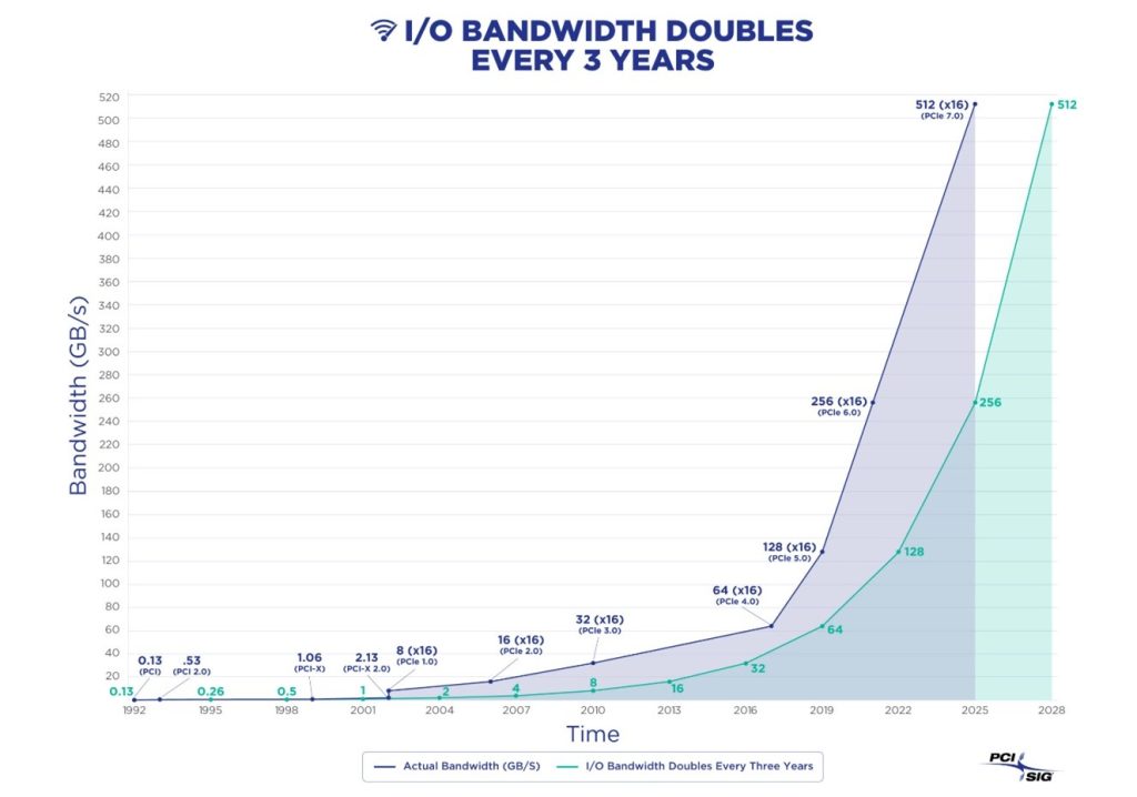
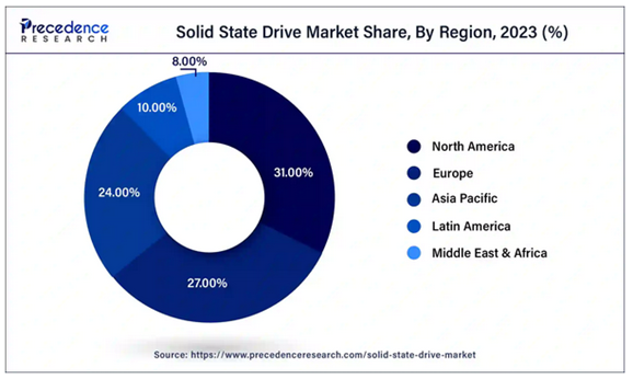
In this project a system was developed, that covers many IPs. Very interesting to see, is the general interest of the industry to these IPs. Although the consortium thought and act in the system context every partner has its own new or extended marked, enabled by this project. The likelihood is high that a commercial product will be based on the realized developments. In this scenario the established partnership can be activated, which will speed up the development. To enable efficient work, an infrastructure was developed and set-up, that manages the data exchange and similar things. This isn’t countable in numbers for market potential but enables a faster time to market. Many things done in this project can be used (with adaptations) in combination with Chiplet technology. The following diagrams show the market forecast for SSD storage, which will be dominated by PCIe based systems. A doubling in the data throughput every 3 years is a fact, that shows the dynamic in this segment. The chiplet approach will enable a modular approach to keep pace with the very fast increase in date throughput.

Societal & Economic Impact
The project opened the chance to establish an SMI-based European network to develop a very reliable, secure and ultra-low power flash memory controller. This chance was taken, and a real partnership was established. This partnership isn’t only related to this project. During the project run-time, but not in the project context, the partners used the special expertise
available in consortium. The online and face to face meetings helped a lot to get a better technical understanding but also to establish new business relationships.
Patents, Standardisation, Publications
Patents:
— “Method and system for error correction based on generalized concatenated codes with restricted error values for code-based cryptography” Patent file number: USA – Germany 10 2021 128 031.1
— “Method and system for read reference voltage calibration for non-volatile memories” Patent file number: USA 17/939,718; Germany 10 2022 209 318.6
Theses:
— “Enhancing Reliability and Efficiency in Flash Memory: Readout Methods and Error Correction Algorithms” D.Nicolas Bailon; Sept. 2024, doctoral thesis, Ulm University
— “The Weight-One Error Channel and its Application in Code-Based Cryptography” J.-P. Thiers; Sept. 2023, doctoral thesis, Ulm University
— 1 master thesis & 4 bachelor theses
Future Developments
With this project a big step technology was possible. Still there is a gap to the competition in ASIA. This means there is further effort and willingness needed to reach the same technology level. Without doing this, only niche markets can be reached, which shouldn’t be the target. Chiplet looks right now a very interesting technology to close the gap, since a scaling is easier doable. The EU has an extreme dependency to data storage solution developed and manufactured in ASIA. To reduce the dependency the Chiplet approach seems a smart way to get the enormous investment managed. Nevertheless, developments in technologies 5nm and smaller are required. The required investments are not doable for SME without substantial funding.
As visible in the diagrams, the demand on storage will increase with the increasing numbers of AI applications. Countermeasures on EU level are needed to avoid a further increase of
the dependency from ASIA. Security aspects are an additional critical aspect to consider.


