Project status :
Recently completed
Project profile (pdf) :
Project impact (pdf) :
Key application areas
 Energy
  Transport and Smart Mobility
  ECS Process Technology, Equipment, Materials & Manufacturing
 Essential capabilities
 Systems and Components Architecture, Design & Integration
Connectivity & Interoperability
 Safety, Security & Reliability
  Computing & Storage
ECS Process Technology, Equipment, Materials & Manufacturing
Computing & Storage
ECS Process Technology, Equipment, Materials & Manufacturing
PARTNER
Besi Netherlands B.V. / CSA Catapult / Cambridge GaN Devices Ltd / Eindhoven University of Technology / Fraunhofer IMS / Infineon Technologies AG / Lyra Electronics Ltd / MACCON Elektroniksysteme GmbH / Neways Technologies BV / SUMIDA Components & Modules GmbH / Signify / TU Dortmund / advICo microelectronics GmbH
Besi Netherlands B.V. / CSA Catapult / Cambridge GaN Devices Ltd / Eindhoven University of Technology / Fraunhofer IMS / Infineon Technologies AG / Lyra Electronics Ltd / MACCON Elektroniksysteme GmbH / Neways Technologies BV / SUMIDA Components & Modules GmbH / Signify / TU Dortmund / advICo microelectronics GmbH
Countries involved
 Germany
  Netherlands
  United Kingdom
 Project leader(s)
Martin ArnoldKey project dates
01 February 2020 - 30 April 2023GaNext project is the development of an intelligent Gallium Nitride (GaN) power module where the drive, control, and protection circuits are integrated or co-packaged with the power device.
GaN transistors are wide-bandgap compound semiconductor devices that revolutionize power electronic systems. They offer lower resistance, faster switching times, and reduced losses compared to silicon devices. GaN enables higher operation frequencies, leading to smaller passive components and more compact power electronic systems. In GaNext, 13 partners collaborated and developed a GaN-based Intelligent Power Module (IPM) integrating drive, control, and protection circuits.
Background, objectives of the project and challenges
GaN is arguably the most promising material to replace silicon in power electronics applications in the 650V market sector. This sector is worth multi-billion with applications ranging from power supplies, power factor correction, AC-DC converters, and wireless charging to inverters in electric vehicles. Power systems based on GaN are lighter, more compact, significantly more efficient and potentially cheaper than those based on silicon. But the high switching speed and low gate voltage of state-of-the-art GaN devices make them challenging to use.The aim of project ‘GaNext’ was to remove the barriers to the adoption of GaN and fully demonstrate the higher efficiency and compactness of GaN-based systems in a range of power systems. The heart of the project was the development of an intelligent GaN power module where the drive, the voltage control, and the protection circuits are integrated or co-packaged with the power device.The new suggested integrated power module addresses some key problems with current GaN-based circuits. Currently, GaN has certain advantages, but its switching speed needs to be slowed down to prevent high-frequency oscillations. This means that users do not fully benefit from GaN’s capabilities. However, by integrating some passive components into the module, GaNext has reduced these oscillations and also decreased electromagnetic interference. Another issue is that the gate voltage distortions can cause unreliable switching of the transistors. But with the tailored design of the GaNext gate driver and its close integration with auxiliary devices on the GaN – Integrated Circuit (IC), these distortions have been minimized and the reliability of switching has been improved. To fully unlock the potential of GaN, a high-speed control IC has also been added with advanced safety features and heat extraction has been implemented. Furthermore, current and temperature sensors have been directly integrated onto the GaN-IC. This allows to significantly expand the safe operating area of the system. Additionally, a dedicated package for the power module has been developed, encompassing the GaN power transistor, control circuitry, and drive circuitry. This module has been successfully demonstrated, providing a competitive advantage in power systems such as Electric Vehicles’ (EV) chargers, lighting, drives, and photovoltaic (PV) inverters, all of which feature optimized magnetic components. By addressing these various aspects, GaNext IPM has become a central component in the next generation of GaN power systems.
Technological achievements
The project aimed to address two main challenges related to GaN adoption and achieved specific outcomes. The key achievements include:
Goal 1: Remove barriers to adoption for GaN
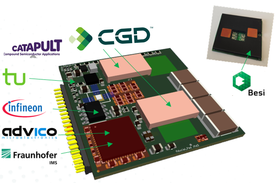
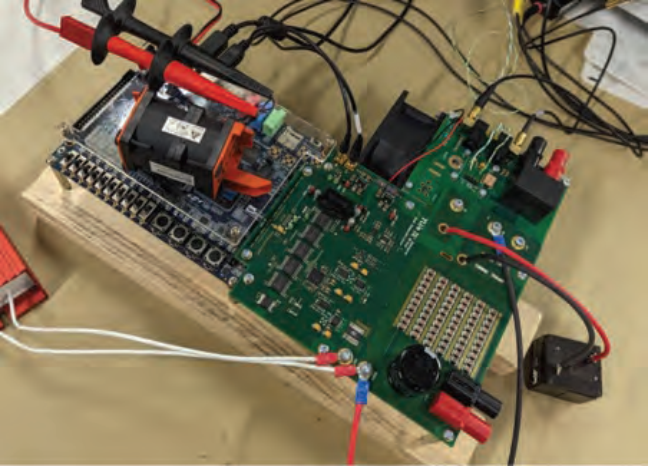
The project successfully built a co-packaged intelligent GaN power module (see Figure 1), which integrated GaN technology into a compact and efficient power module design. This achievement aimed to overcome challenges such as limited knowledge, high costs, and complex integration associated with GaN adoption.
Goal 2: Demonstrate higher efficiency and compactness of GaN-based systems
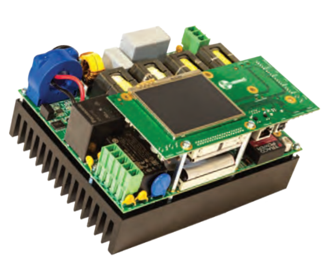
The project successfully demonstrated the higher efficiency and compactness of GaN-based systems in a range of power systems (Figure 2). This achievement validated the potential benefits of GaN technology, including improved energy efficiency and reduced size of power electronics.
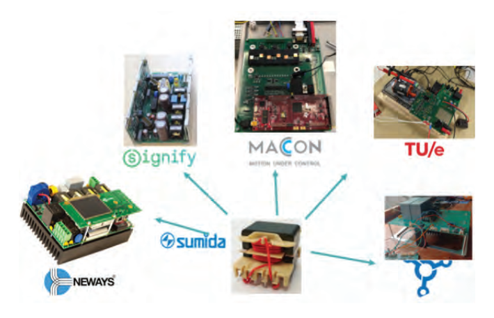
Signify developed the Horticulture driver,MACCON developed a motor drive demonstrator, TU/e developed High-Frequency Modulation Strategies and Lyra developed the prototype on-board charger.
GaNext made breakthroughs in four main areas.
1. GaN-on-Si power Integrated Circuit (IC) (650V, up to70A) with integrated sensing and driving elements.
2. Si and GaN low-voltage logic, control, and level-shiftSilicon-on-Insulator (SOI) gate drive circuitry.
3. Manufacturing of a dedicated package for the powermodule that included the GaN power transistor andthe control and drive circuitry.
4. Demonstrated competitive advantage of the powermodule in power systems such as EV charger,lighting, drives and PV inverter; featuring optimisedmagnetic components.
Key Achievement by Project Partners
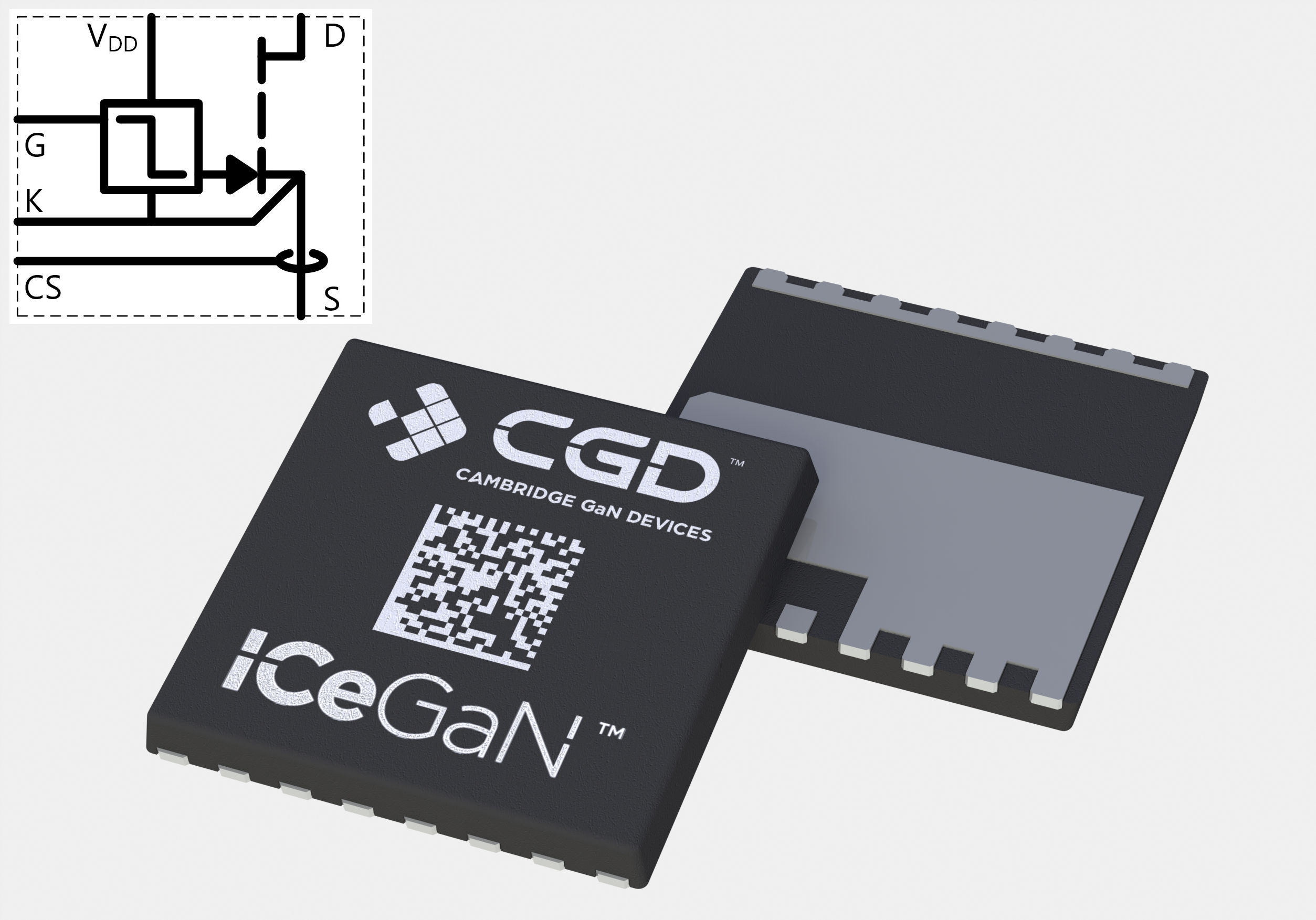
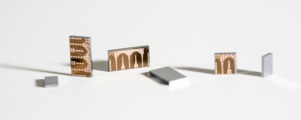
Cambridge GaN Devices (CGD) 55mR chip has been qualified as per JEDEC standards (Figure 3, left). The Cu and back metallization of GaN devices developed in GaNext (Figure 3, right) has enabled CGD to serve markets that need GaN devices integration in the Intelligent Power Module (IPM).
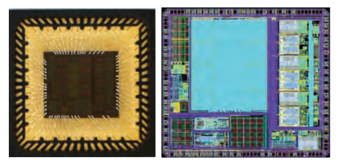
Infineon developed an Optimized Gate Driver Testchip with enhanced SOI technology, featuring 50% less propagation delay (45ns vs. 90ns), 2X driving capability, 19% design shrink, increased breakdown voltage (700V), superior Electro-static Discharge (ESD) performance (above 2kV), and lower costs for module assembly (IPM)Fraunhofer IMS and Advico developed a High Resolution Digital Pulse Width Modulation (PWM) Controller (Figure 4) with integrated power management, feedback channels, a programmable 32-Bit RISC-V safety core, and an AI hardware accelerator interface. It also offers functional safety functions, external hardware interfaces, and a selectable digital communication interface.
In the GaNext project, TU Dortmund (TUDo) developed alpha and beta versions of circuit boards. The alpha versions have 4 layers and filled vias, while the beta versions have 6 layers, filled buried vias, and include a microcontroller. The iFF circuit’s efficiency was demonstrated with alternative boards, resulting in a 50% reduction in switching losses. The comparison showed slight improvement with parallel connected gate drivers.
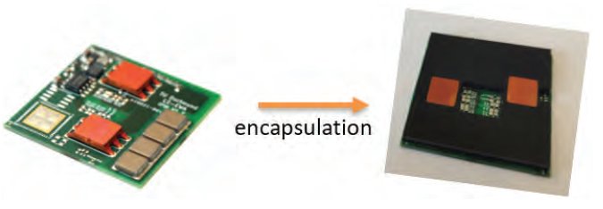
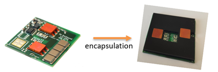
Besi demonstrated encapsulation of a IPM containing GaN technology with novel high thermal conductive epoxy molding compounds (Figure 5)
The CSAC’s involvement in the project supported the gaining of deeper knowledge about boot-strapped gate drivers, designing a thermal resistance test rig, developing a dynamic thermal impedance characterization system, creating a GaN double-pulse test rig with a GUI, and designing a resonant test PCB (Figure 6) for high power functional tests.
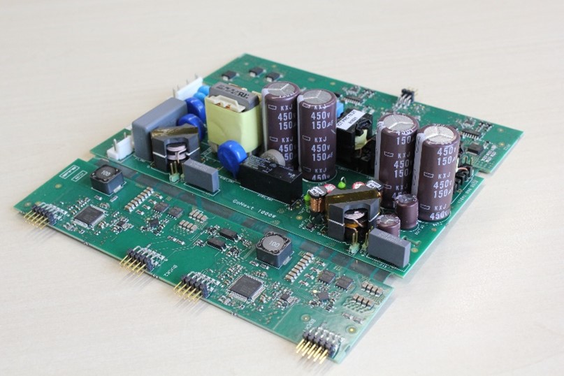
SUMIDA developed custom magnetic components for a wide range of applications, including automotive and industrial. They worked closely with partners to develop advanced and optimized components that meet power application needs. An example is their magnetic development with Neways for PV inverter (Figure 7).
Lyra designed and developed a prototype of GaN based Dual Active Bridge (Figure 8) with High speed PWM control software, operating at 5kW, ~400V, and with a Soft switching algorithm.
Signify developed a Buck Converter with GaN-based Horticulture (Figure 9). It reduces driver size by 30% and enables the use of 600V GaN technology with 400Vac mains. The output stage switches at 1-2 MHz using GaN technology, resulting in smaller magnetic components. It incorporates advanced digital control, new PCB techniques to reduce noise and EMI, and a semi-flex PCB design for higher volume utilization.
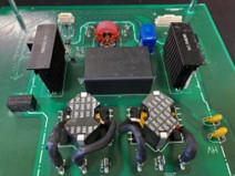
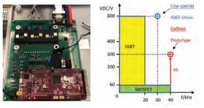
MACCON has developed drives that expand the voltage range of their 40kHz inverter portfolio by a factor of 5 (Figure 10). They achieved this by introducing a GaN Half-Bridge module that utilizes discrete components. Additionally, they have designed a Universal Mainboard that supports the IPM and the MACCON Module.
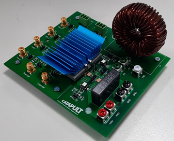
The Eindhoven University of Technology (TU/e) has developed strategies to increase the switching frequency of power converters using GaN technology (into the megahertz range). This enables smaller, cheaper, more efficient converters. They employed new modulation strategies and real-time state observers for variable frequency operation with zero-voltage switching. A 3kW demonstrator (Figure 11) was created to test and verify the performance of these techniques, including cooling concepts.
Neways has developed a 3kW PV inverter technology demonstrator (Figure 12) with a high efficiency (up to +/- 99.2% for the boost stage) in a small form factor (312W per litre). It can beneficially be used to reduce the total cost of ownership on the application level, increase the efficiency of applications, and downsizing existing applications
Market Potential
Besi gained valuable insights through GaNext, facilitating the design of advanced GaN-based IPM packages with exceptional thermal performance for the GaN power market. CGD utilized GaNext to establish a comprehensive supply chain, enabling compatibility with advanced packaging technologies and positioning themselves in the bare-die business. Infineon holds the second position in the gate driver IC market, leveraging optimized SOI technology to strengthen its presence in established applications and penetrate new markets. Their gate driver ICs, enhanced with optimized SOI technology, drive the adoption of Wide Band Gap (WBG) GaN and SiC semiconductors, expanding their share in the IPM market. Neways, an EMS supplier, is well-positioned to benefit from the demand for power electronics in the e-mobility and automotive sectors. The growing e-mobility charging market offers an opportunity for Neways to differentiate with GaN IPMs. Signify dominates the Horticulture market, delivering innovative lighting solutions. These companies are poised to capitalize on industry trends, technological advancements, and market growth, ensuring their competitive advantage and driving success in their respective markets.
Societal & Economic Impact
The GaNext project has significant societal and economic impacts. It has closed the technology gap in GaN module manufacturing, enabling the faster and simpler design of high-performance power electronics. This disruptive approach has given European companies a competitive edge, increasing their market penetration and strengthening the European electronics market. GaNext fostered collaboration among companies and supported the creation of an integrated European GaN chain. The project aligned with clean growth missions, reducing of carbon emissions, and improving energy efficiency. It supported inverterization of home appliances, increasing energy savings. GaNext’s advancements in power electronic modules for drive train electrification lead to higher efficiency, lower costs, and increased reliability. It also contributed to the development of sustainable horticulture, enhancing lighting systems for energy-efficient cultivation. The publicly available GaNext open source components, including the AIRISC RISC-V processor, have garnered significant interest among academic users. These components have already found applications in radiation-resistant DC/DC controllers for the CERN ATLAS experiment and have been utilized in research focused on developing efficient AI hardware. GaNext’s development of higher-efficiency power converters with a compact footprint is a notable achievement. These converters offer cost-effective solutions and potential affordability compared to existing options. They contribute to energy savings, reduced environmental impact, and the adoption of renewable energy sources.Overall, GaNext pushed for innovation, competitiveness, clean growth, and sustainability across industries. GaNext’s intelligent GaN-power module demonstrator facilitated solutions for reducing carbon emissions and improving energy efficiency. They support sustainability goals and enhance the quality of life for future generations.
Patents, Standardisation, Publications
GaNext dissemination efforts have included:
— Acquisition of 7 valuable grantedpatents (with more in the publication stage)
— Release of 7 informative pressreleases
— Participation in 13 conferences(such as PCIM, APEC, Electronica etc.)
— Publication of 4 research papersin prestigious journals (with more in progress)
— Coverage in 5 renowned magazines
— Completion of 5 theses(4x Bachelors & 1x Masters)
— Garnering over 18,000 websiteviews along with a strong presence on LinkedIn
These endeavors collectively showcase the project’s commitment to widespread knowledge sharing and impactful contributions to the field.
Future Developments
Besi and Neways will participate in “R-Podid”. Besi will further investigate the influence of encapsulation on GaNbased power module reliability. CGD’s collaboration with CSAC has impacted product development, including the dv/dt immunity improvement circuit and thermal characterization in the UK-funded project “P3EP.” Infineon leverages project results to enhance gate driver IC derivatives and expand the Level Shifter and IPM portfolios. Memorandum of Understanding signed between Neways-CGD on further enhancement of future collaboration. Signify develops GaNbased Horticulture drivers and conducts research in projects like PowerizeD and All2GaN. TUDo focuses on iFF circuit development and reliability testing, comparing multiple setups. TU/e will develop a power electronics building block using ALL2GaN techniques, studying WBG device reliability. FHG secured internal funding to advance the TRL of the AIRISC-POWER processor to TRL5, following successful outcomes in GaNext. To aid the development process, an advisory board led by Siemens and X-Fab has been established by FHG.

