Project status :
Completed
Project profile (pdf) :
Project impact (pdf) :
Key application areas
 Health and Wellbeing
  Connectivity
 Essential capabilities
 Components, Modules and Systems Integration
Connectivity
Components, Modules and Systems Integration
Connectivity  Process Technologies, Equipment, Materials and Manufacturing
PARTNER
Capical GmbH / Fraunhofer EMFT / IMS CHIPS - Institut fuer Mikroelektronik Stuttgart / Integer / Irish Manufacturing Research / NanoWired GmbH / OSYPKA AG / Philips Electronics Nederland BV / Philips Healthcare / Reden BV / Salvia BioElectronics BV / Schmoll Maschinen GmbH / Signify / TNO / Technische Universität Dresden / Würth Elektronik GmbH & Co. KG
Capical GmbH / Fraunhofer EMFT / IMS CHIPS - Institut fuer Mikroelektronik Stuttgart / Integer / Irish Manufacturing Research / NanoWired GmbH / OSYPKA AG / Philips Electronics Nederland BV / Philips Healthcare / Reden BV / Salvia BioElectronics BV / Schmoll Maschinen GmbH / Signify / TNO / Technische Universität Dresden / Würth Elektronik GmbH & Co. KG
Countries involved
 Germany
  Ireland
  Netherlands
 Project leader(s)
Volker Franco SteierKey project dates
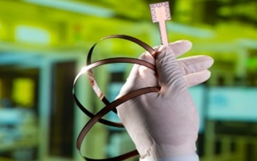
April 2022- March 2025The HyPerStripes project extended the limits of roll-to-roll (R2R) metal patterning of flexible/stretchable substrates and developed assembly methods for such substrates.
Printed circuit boards (PCB) are commonly used in the electronics sector to enable miniaturization of products, avoid expensive wire solutions, and reduce assembly effort and costs. However, the technology is currently limited in size and is typically used with non-elastic materials. To use PCBs in other technological sectors, existing limits must be overcome in a cost-effective and sustainable way.
Achievements and results of the project
Thanks to the development of innovative roll-to-roll (R2R) techniques, extra-long elastic PCBs can now be manufactured. Tailored assembly technologies are now also available to connect electronic components to flexible PCBs. Due to the developed technologies and the strong cooperation between the partners in the project, three medical and two industrial product demonstrators were built up in the project. The initiated developments will be further improved, to provide operational manufacturing
processes and innovative products for industrial applications.
Background, objectives of the project and challenges
Elastic PCBs are usually made with sheet-to-sheet (S2S) technology, which allows maximum sizes up to 640 mm x 480 mm. However, this technology could be used on a
much larger scale, if the dimensional restriction did not exist. Existing roll-to-roll (R2R) technology could be adapted so that flexible and elastic substrates can be manufactured in a continuous way and therewith generate almost endless PCBs. Applying this technology could further reduce manufacturing costs, the required raw material and thus greatly expand the use of PCBs in other technological areas.
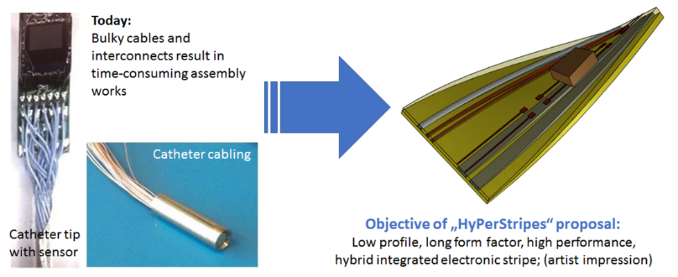
To show the benefits, we chose two industrial areas that would benefit greatly from long, flexible PCBs: the lighting and the medical industry. Examples from both sectors were generated and are shown later. Besides the flexible PCBs themselves, there is a need for specialized assembly technologies to equip long strips with sensors, lights, passive components, or smart components.
Due to the limitations and advantages described, the main goal of the HyPerStripes project was to develop:
- Assembly technologies tailored to the R2R processes.
- R2R manufacturing technology for flexible and elastic PCBs.
To verify the technological advances, five usage examples (uc) from the medical and lighting sectors were developed, built, and tested during the project. These examples show that the use in the respective field is beneficial. Another goal was to create a technology platform where interested customers can stay updated on the project’s
progress and connect with related partners.
Technological achievements
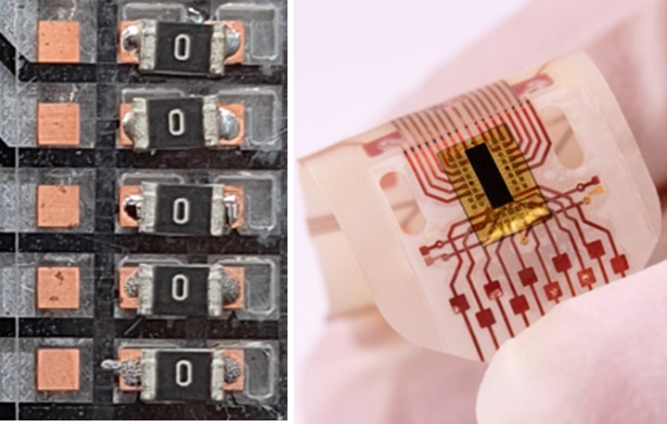
In the project, two different R2R processes were put into operation. The first process uses screen printing and was tested on flexible polymer substrates and conductive traces (Fig. 2).
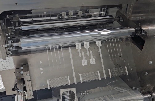
The second process is based on digital lithography and was tested on flexible/stretchable substrates with copper traces (Fig. 3).
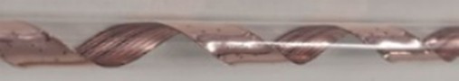
To transform the manufactured PCBs into uc, different assembly steps were necessary (PCB to PCB/components/connectors etc.). Two novel assembly technologies, which were developed for, or rather adapted to the R2R processes.
— Pixel soldering: An assembly technique, which increases temperature only in small target areas enables local soldering. Thereby, intense temperature loads in large areas can be avoided (Fig. 4, left).
— NanoWiring: A technology that simplifies work like a Velcro-Closure and can be used to connect PCBs or chips. The process grows fine metallic needles on predefined conductive areas. Within the project, a concept to adapt the technology for R2R-applications was developed (Fig. 4, right).
left: pixel soldering, TNO
right: NanoWiring, Nanowires
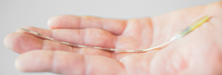
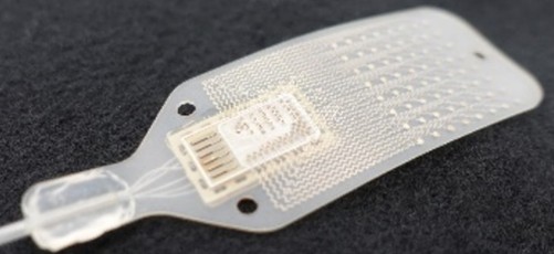
The described technologies were used to build up five uc. Philips developed a concept to substitute traditional wiring in catheters by spirally twisted PCBs (Fig. 5).
Salvia tested the printed stripes to verify their possible use as active nerve-stimulating implants to treat severe migraine patients (Fig. 6).
OSYPKA developed and built up an active implant demonstrator, equipped with an electrode array and encapsulated micro controller, that can digitalize the recorded signals close to the electrodes (Fig. 7).
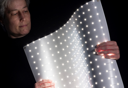
Signify used transparent and with LEDs assembled HyPerStripes to build windows that can, transform into opaque luminary (Fig. 8).
Capical used flexible PCBs in intelligent bed sheets that constantly monitor body signals. The developments were supported by simulations in the thermal, electrical and mechanical domains. The developed design process simulation toolchain will be made available to the public on an open-access simulation platform (github.com/IFTE-EDA/ftl). Further information as well as direct contact to the involved partners can be found on hyperstripes.ims-chips.de.
Market Potential
The project consortium targets three different market sectors, wherefore the market potential will be described selectively. All three sectors have a global market volume in the multi-billion euro range, flexible electronics 27 B€, medical devices 550 B€ and lighting 80 B€. The growth rate for all the sectors is estimated to be between 9 % and 12%, indicating highly promising forecasts. Even though the actual numbers and forecasts are promising, Europe continues to lag behind in global comparison. The technologies discussed above allow production in Europe. This underlines the need for innovative technology and product developments to remain competitive. Besides the consumer
markets addressed within the consortium, further Industrial applications in high-performance sectors like automotive, customer electronics (cellphones, tablets) and aviation will follow, and thus provide an optimal basis for the implementation of the developed technologies and products.
Societal & Economic Impact
Sustainable design principles were embraced in the design across the different uc and the life cycle assessment of the demonstrators showed great promise. To highlight the biggest possible emission savings, the use of HyPerStripes for lighting solutions can reduce emissions by up to 65% compared to traditional production. The assembly technologies investigated (nanowiring/pixel soldering) also showed emissions reduction potential above 90%. The implementation of circular economy principles across
materials for manufacturing and end-of-life treatment of products can unlock additional improvements.
Patents, Standardisation, Publications
Intellectual property related to the application of Nanowired technology within the R2R manufacturing process, was generated. Furthermore, the project results were presented in two online webinars, eleven talks at conferences and seminars, four conference presentations, two conference posters and one peer-reviewed publication. The results were also presented at eight fairs all over the globe and presented to selected customers by industrial partners. The dissemination activities are continuing, and similar performance numbers are expected for the year after the project.
Future Developments
Both the technological and the application-oriented partners are committed to continuing the initiated developments and aiming to bring the generated results to broadly
utilizable technologies and products. To enable continuous development, the consortium seeks for further financial support through a project application to a Xecs 2024 call (Project name: Multistripes). The consortium remains confident in the economic relevance of the technology and its applications. The developments achieved are expected
to be integrated into future production sites and products.

